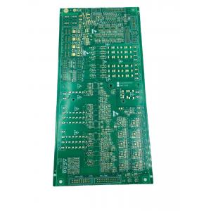
FR4 2-layer board, solder mask green oil, surface immersion gold
Here are some details about the FR4 2-layer board with a green solder mask and surface immersion gold:
The board is made of FR4 material, which is a common glass-reinforced epoxy laminate material that is widely used in PCB manufacturing.
The board has two layers, which means that it has two layers of conductive material separated by an insulating layer. Two-layer boards are often used in simpler circuits or where cost is a concern.
The board has a green solder mask, which is a type of protective coating that is applied to the board to protect the copper traces and prevent solder bridges. The green color is a standard color used in PCB manufacturing.
The board has a surface immersion gold finish, which is a type of surface finish that provides a flat and even surface ideal for soldering. The immersion gold finish also protects the copper traces on the board from oxidation and corrosion.
Overall, this FR4 2-layer board with a green solder mask and surface immersion gold is a standard board that is designed for simple circuits or where cost is a concern. The board has been coated with a green solder mask to protect the copper traces and has been finished with an immersion gold surface to provide a reliable and corrosion-resistant contact surface for external connections.
| Item | capability |
| Base Material | FR-4, High TG FR-4 , Halogen Free material ,CEM-3,CEM-1,PTFE,Rogers ,Arlon ,Taconic,Aluminum base,Teflon,PI ,etc |
| Layers | 1-60 |
| Finished inner/outer copper thickness | 0.5-6OZ |
| Finished board thickness | 0.2-7.0mm(≤0.2mm needs review),≤0.4mm for HASL |
| | Board thickness≤1.0mm: +/-0.1mm
1Board thickness>2.0mm: +/-8% |
| Max panel size | ≤2sidesPCB: 600*1500mm
Multilayer PCB: 500*1200mm |
| Min conductor line width/spacing | Inner layers: ≥3/3mil
Outer layers: ≥3.5/3.5mil |
| Min hole size | Mechanical hole: 0.15mm
Laser hole: 0.1mm |
| | Drilling precision: first drilling First drilling: 1mil
Second drilling: 4mil |
| Warpage | Board thickness≤0.79mm: β≤1.0%
0.80≤Board thickness≤2.4mm: β≤0.7%
Board thickness≥2.5mm: β≤0.5% |
| Controlled Impedance | +/- 5 % Ω(<50Ω),+/-10%(≥50Ω),≥50Ω+/-5% (needs review) |
| Aspect Ratio | 15:01 |
| Min welding ring | 4mil |
| Min solder mask bridge | ≥0.08mm |
| Plugging vias capability | 0.2-0.8mm |
| Hole tolerance | PTH: +/-3mil
NPTH: +/-2mil |
| Outline profile | Rout/ V-cut/ Bridge/ Stamp hole |
| Solder mask color | Green,yellow,black,blue,red,white,matte green |
| Component mark color | white,yellow,black |
| Surface treatment | OSP: 0.2-0.5um
HASL: 2-40um
Lead free HASL: 2-40um
ENIG: Au 1-10U’’
ENEPIG: PB 2-5U’’/ Au 1-8U’’
Immersion Tin:0.8-1.5um
Immersion silver: 0.1-1.2um
Peelable blue mask
Carbon ink
Gold plating: Au 1-150U’’ |
| E-Test | Flying probe tester : 0.4-6.0mm,max 19.6*23.5inch |
| | Min spacing from test pad to board edge : 0.5 mm |
| | Min conductive resistance : 5 Ω |
| | Max insulation resistance : 250 MΩ |
| | Max test voltage : 500 V |
| | Min test pad diameter : 6 mil |
| | Min test pad to pad spacing : 10 mil |
| | Max test current : 200 MA |

Shenzhen Jieteng Circuit Co., Ltd. is a reliable and reputable PCB manufacturer with a strong focus on quality and innovation. The company utilizes advanced manufacturing equipment and techniques to ensure its PCBs meet the highest standards. The company has a team of experienced engineers and technicians who work closely with customers to ensure that our PCBs meet their specific requirements.
Along with its commitment to quality, the company is also committed to providing excellent customer service. Jeton Circuit Co., Ltd. works closely with customers to provide personalized solutions and support throughout the entire PCB manufacturing process from design to delivery.